Leading the future with breakthrough SPAD technology
Discover how our state-of-the-art SPAD technology is transforming the industry. Dive into the future with us!
Transforming optical imaging: the power of SPAD technology
Pi Imaging is a leading innovator in the field of optical imaging, revolutionizing light detection through our single photon avalanche diode (SPAD) technology. We use SPADs because they offer unprecedented image quality in low-light, high-speed, high-dynamic range and time-resolved applications.
To enable the above applications, we need to introduce operational and architectural changes in detection and accumulation of photo-electrons. Opposed to accumulating photo-electrons in a fragile environment with thermal and other analog noise sources, as it is done in analog PMT detectors, EMCCD and sCMOS imagers, photons can be counted by means of a direct photon to digital transformation. Simplified, this marks a transition from analog to digital light detection.
Operating in the digital domain increases the robustness of detecting extremely weak light signals, photons, and allows for extreme imaging speeds. This translates to both high frame rates, high-dynamic range and time-resolved detection.
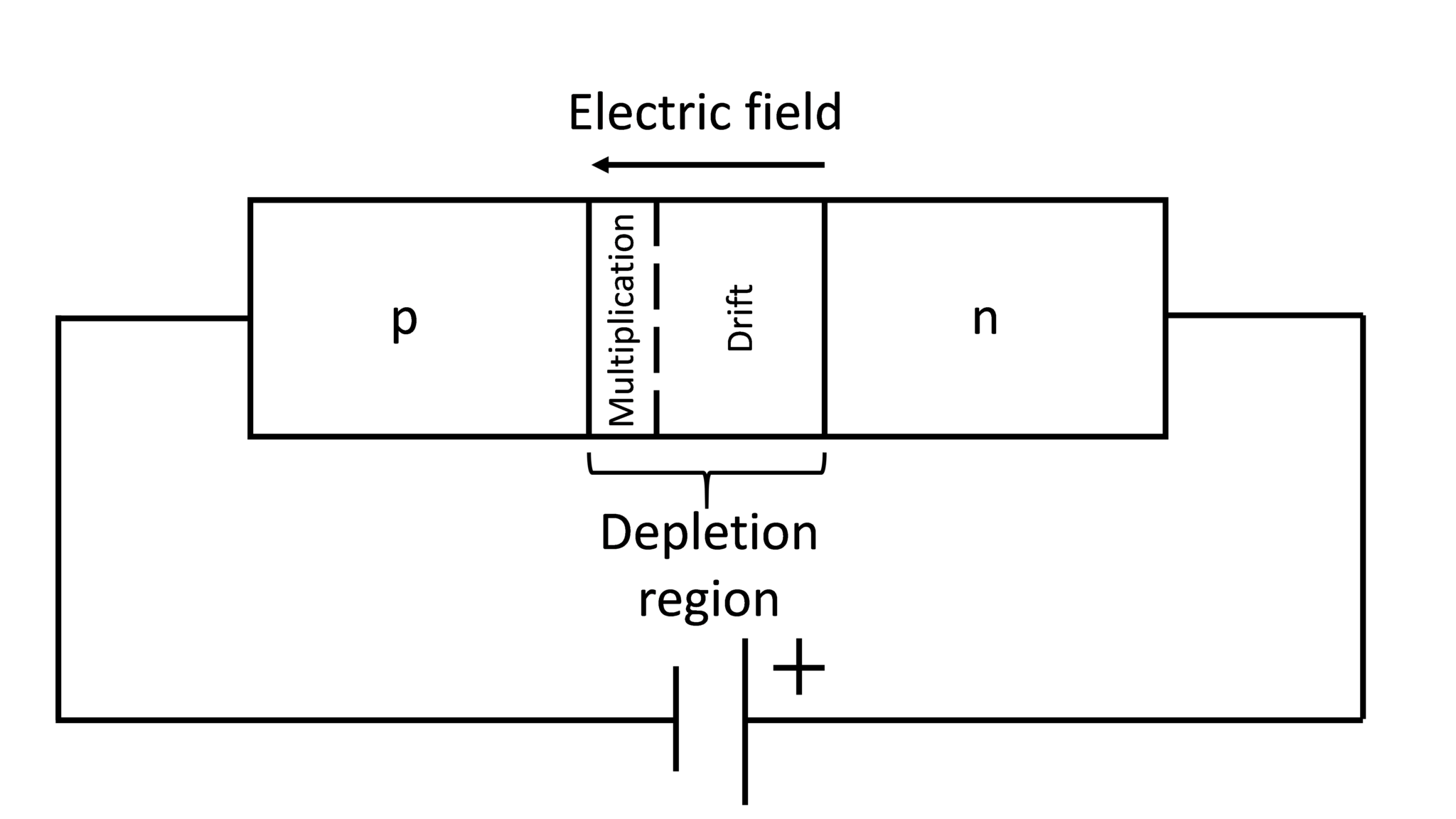
Figure: Reverse-biased photodiode. We create a depletion region at the p-n junction by applying a reverse bias. At high reverse bias, a multiplication region is formed closer to the more doped layer (in this case the p layer), where carriers are accelerated (and multiplied) to create an avalanche. Photons absorbed in the drift region are creating avalanches after drifting towards the multiplication region.
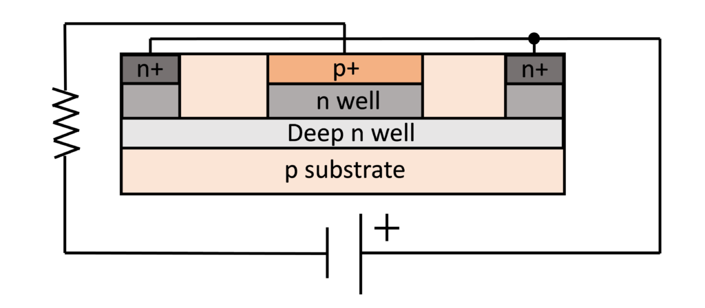
Figure: A typical implementation of a SPAD in a standard CMOS process, with a ballast resistor in series. The depletion region is in this case formed between the p+ and n well layers. The side and bottom n layers are used for connectivity with the n well.
What is a SPAD?
A SPAD is a photodiode that is capable of triggering electrical avalanches upon detection of a photon. The generic structure of a SPAD is shown in the following figure. Photons are absorbed (generating an electron-hole pair) by the semiconductor lattice (silicon or other semiconductors). The electric field of the depletion dipole generates current if the photons are absorbed close to the depletion layer.
A high electric field creates current avalanches if SPADs are operated above breakdown voltage VBD, at the operating voltage VOP=VBD+VE (VE is the excess bias). Above breakdown, electron-hole pairs are abruptly accelerated and generate impact ionization. The SPADs then operate in so-called Geiger mode, where a detected photo-electron generates an avalanche. In passive quenching regime, the avalanche current is quenched by a ballast resistor. The same resistor is used to sense the current by generating a fast voltage pulse, thus we achieve a photon-to-digital converter. A SPAD usually comprises a junction between a highly doped p+ layer and an n well, shown in figure below.
SPADs can be successfully integrated in large arrays since they are very similar to standard microelectronic chips fabricated in complementary metal-oxide semiconductor (CMOS) technology. In fact, SPADs can themselves be fabricated in standard CMOS and CMOS image sensor (CIS) technologies.
SPAD pulses usually have a rising edge of a few nanoseconds and a jitter of 100 ps; the pulse width is between 10 and 100 ns. This implies that at most one photon can be detected every 10 to 100 ns. The maximum imaging speed in these cases is thus 400 kfps (or 40 kfps in case of 100 ns dead time) for a single measurement with 255 different gray values (from black to white) assuming accumulation of subsequent pulses is used to form the gray levels.
SPAD imagers are arrays of SPADs that enable high timing resolution and are thus suitable for time-resolved and high-speed applications. For example, a distance can be measured implicitly by the time taken by light to travel from a laser source to an object and back to the detector. Inherently, SPAD imagers have a high photon response uniformity and zero readout noise.
History of the
SPAD arrays
SPADs (single photon avalanche diodes) were first developed in the 1970s, but it wasn’t until the early 2000s that they began to be used in commercial applications. Europe was the epicenter of academic SPAD development.
In 2002, Prof. Edoardo Charbon joined EPFL (Swiss Federal Institute of Technology in Lausanne) and began focusing on SPAD arrays built in standard semiconductor flows (CMOS). In 2006, a key EU project was awarded to Charbon, indirectly leading to massive commercialization of SPADs in proximity sensors into smartphones.
In 2018, Pi Imaging Technology (PIT) was founded as a spin-off from EPFL, based on the research work of Prof. Charbon, Dr. Claudio Bruschini and Dr. Ivan Michel Antolovic. In 2019, the Pi Imaging team co-developed the world’s first prototype megapixel SPAD image sensor. In 2021, Pi Imaging released the world’s first SPAD-based camera.


Why SPAD arrays and image sensors
SPADs possess several notable characteristics that make them highly effective in targeted applications.
SPADs exhibit an exceptionally high signal-to-noise ratio in low light conditions, making them ideal for detecting and measuring faint light signals. This capability is of particular value when combined with the high-speed digital readout. The high sensitivity of SPADs allows them to discern and distinguish individual photons, enabling the accurate detection and quantification of exceedingly weak light sources.
Due to their nonlinear response to light, SPADs offer extremely high dynamic range.
SPADs have incredibly precise timing capabilities, characterized by a low standard deviation. This feature enables them to measure the time of arrival of individual photons with remarkable accuracy.
Start your project today!
Why Pi Imaging
Best-in-class sensitivity
We combine specialized semiconductor technology with micro-optics to enable the best-in-class SPADs with >50% peak sensitivity and a wide detection spectrum, Poisson (shot noise) limited detection.
Detector array instead of single pixel
Instead of relying on a single pixel, our detector provides an array, enabling image acquisition without scanning.
Extremely high speed
We offer frame rates up to 100’000, 550’000 and 2’000’000 fps our image sensors, line sensors, and point sensors, respectively.
Time tagging 20 ps resolution
Our detector system incorporates advanced time tagging electronics. This feature enables the precise measurement of the arrival time of each detected photon with a resolution of 20 ps.
Access to all the sensor’s functionality
Moreover, to our researchers, we offer low level access to our sensors, which facilitates further application development.
High photon count rate
Pixel parallelization enables the simultaneous detection and processing of numerous photons, increasing the photon count rate compared to traditional single-pixel detectors.
Compact size
This compact design makes it an ideal choice for space-constrained applications where miniaturization is essential. The small footprint of the detector allows for seamless integration into various setups and devices.
